
![]()
Electron microscopy to reveal internal structural properties of laser printed inorganic nanoarchitectures
Contact: Kristian Kraft, Prof. Dr. Yolita Eggeler
Newly developed printing techniques of metallic conductors and whole functional devices [1] have been established in recent years. The printing by laser or inkjet printer allows to create structures in the microscale. Printing such devices benefit from low production costs and high production speeds.
Electron microscopy is used to characterize these printed devices [2] on their micro- and nanoscale [4], as well as their electrical properties [3]. In situ scanning electron microscopy (SEM) allows electrical probing possibilities. With dual focused ion beam (FIB)-SEM the devices are prepared for investigations in transmission electron microscopes (TEM) in order to analyze their local chemical compositions and bonding states using scanning transmission electron microscopy ((S)TEM) and high-resolution transmission electron microscopy (HRTEM) in combination with spectroscopy such as energy-dispersive x-ray spectroscopy (EDXS) and electron energy loss spectroscopy (EELS).
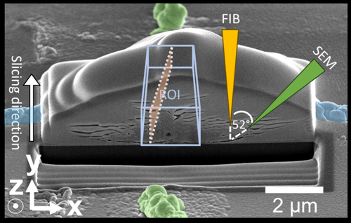
Such devices under investigation are memristors (shown in Figure 4a). Memristors are characterized by the fact that their resistance depends on the voltage that was applied to the component in the past. By applying a positive voltage on the silver electrode and ground on the platinum electrode, a conductive filament is formed in the zinc oxide between the two electrodes (shown in Figure 4b). FIB-SEM tomography is performed to fully describe the Ag distribution in memristors that have experienced electrical characterization (cycled memristor) and non-cycled memristors. For tomography, a protective Pt layer is deposited on the memristor (Figure 5) and a trench is cut in front. From above, slice by slice is removed with the FIB and under an angle with the SEM the region of interest (ROI) is imaged. The reconstructed 3D movies from the 2D images are shown in Movie 2a for the cycled and in Movie 2b for the non-cycled memristor. An important finding is that due to the electrical characterization Ag (in green) accumulates around the lower Pt electrode. In further 3D reconstruction experiments, the aim is to map the conductive Ag filaments responsible for the conduction mechanism.
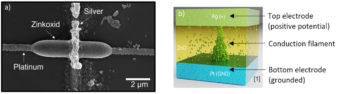
and the Pt. b) Scheme of conductive Ag filament in the ZnO. Here, a ground potential is applied to Pt and a positive potential is applied to Ag top electrode
for the forming process.
is marked in blue and the Pt electrode in green. The ZnO is located under the
protective Pt layer. 3D reconstruction is performed from the ROI. With the FIB, slices
are removed from the top and the SEM images are taken at an 52° angle.
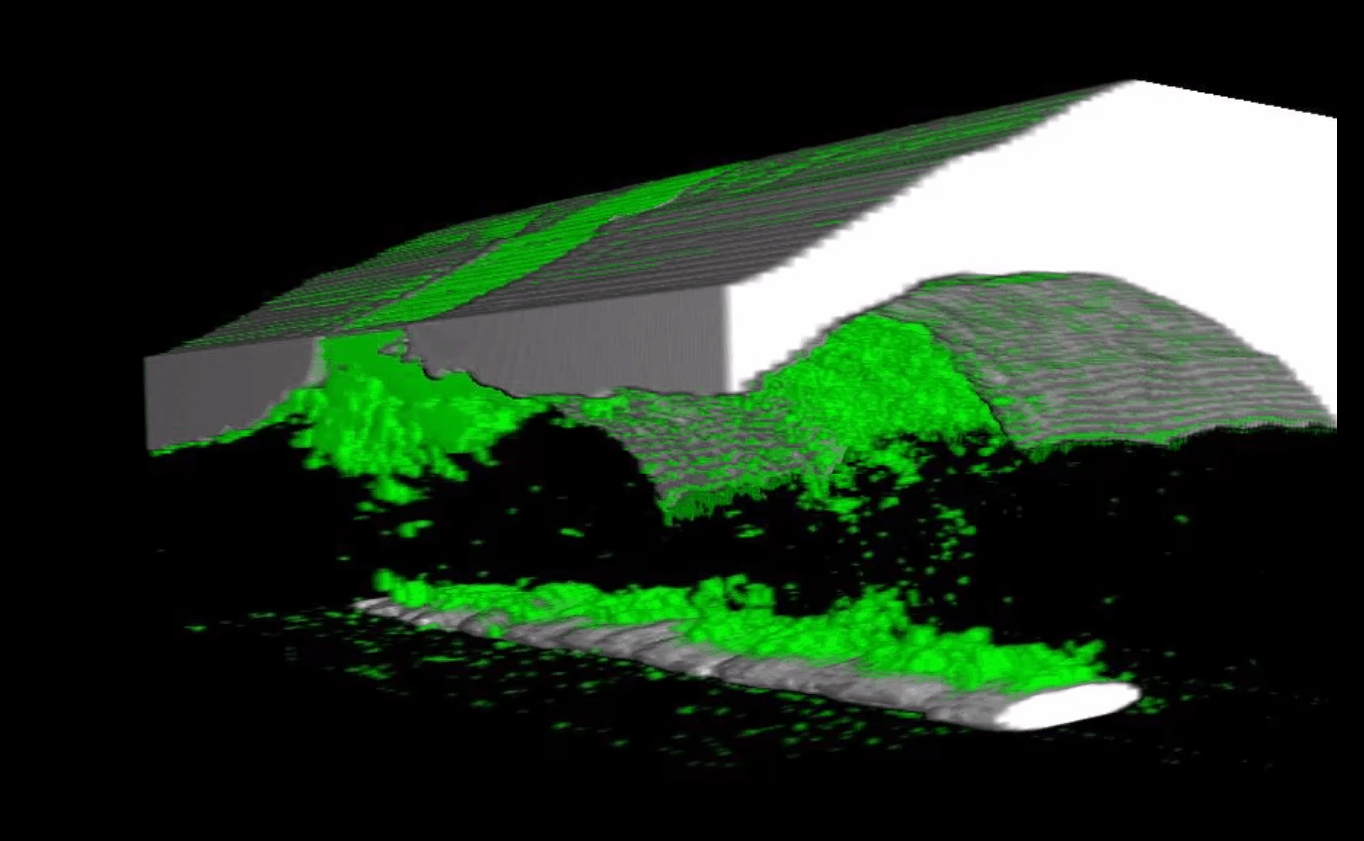
The Ag is shown in green and Pt in white.
Ag is distributed at Pt bottom only for the
cycled memristor. The Ag top electrode
is located under the protective Pt layer.
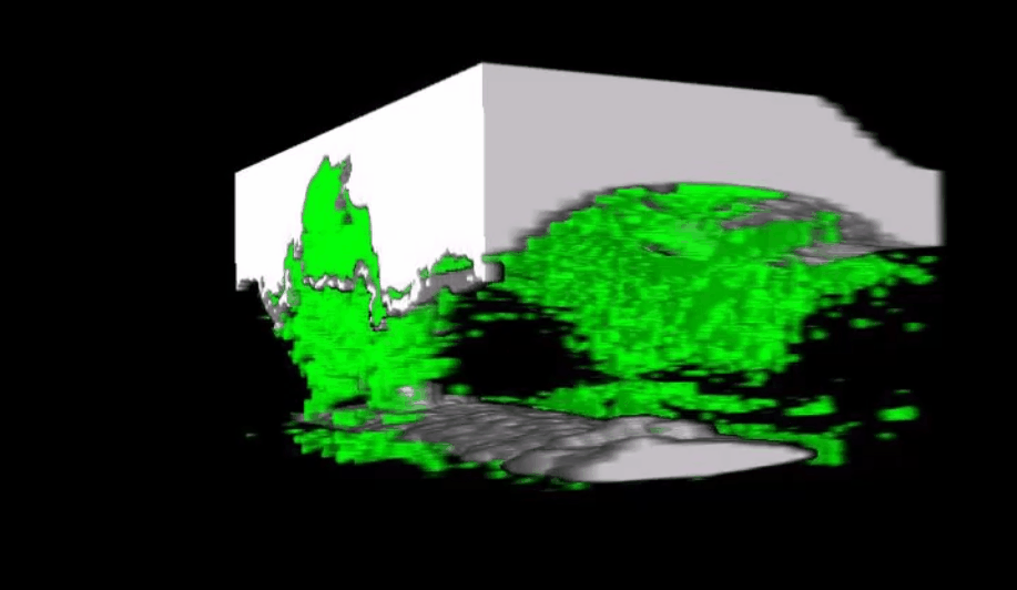
The Ag is shown in green and Pt in white.
Ag is distributed at Pt bottom only for the
cycled memristor. The Ag top electrode
is located under the protective Pt layer.
The aim of a further investigations is to gain a deeper understanding of the scaling parameters on the performance of the printed conductive devices and the formation and conduction mechanisms in the structures [5]. Furthermore, the influence of crystallinity, orientations and internal defects on the printed metallic structures is investigated. Diffraction techniques such as electron backscatter diffraction (EBSD) is used for this purpose. The special feature of the EBSD experiments is that the printed structures are polished with the FIB on the micrometer scale and at a very high angle. Here, printed ZnO single crystals are examined, in which a rotation of the crystal can be observed.
Another research area is dedicated to the development of a lateral memristor design in which material changes are visualized and the resulting switching mechanism [6] by external electrical stimulation in in situ SEM is observed. The aim is to observe in situ the formation of a conductive filament in a memristor.
References
[1] Yang, L., et al. (2023). "Laser Printed Microelectronics." Nature Communications 14(1): 1103.
[2] Hu, H., et al. (2023). "A Fully Inkjet-Printed Unipolar Metal Oxide Memristor for Nonvolatile Memory in Printed Electronics." IEEE Transactions on Electron Devices 70 (6): 3051–3056.
[3] Hu, H., et al. (2021). "Inkjet- Printed Bipolar Resistive Switching Device Based on Ag/ZnO/Au Structure." Appl. Phys. Lett. 119(11): 112103.
[4] Sun, Q. et al. (2023). "In Situ Pyrolysis of 3D Printed Building Blocks for Functional Nanoscale Metamaterials." Advanced Functional Materials: 2302358.
[5] Hu, H. et al. (2023). "Inkjet-Printed Tungsten Oxide Memristor Displaying Non-Volatile Memory and Neuromorphic Properties." Advanced Functional Materials: 2302290.
[6] Yi, H. et al. (2020). "Coexistence of Digital and Analog Resistive Switching Behaviours in Ag/CuAlO2/TiO2/P++-Si Memristor." Journal of Physics Conference Series: 1637(1): 012053.